Polycrystalline Micron Diamond
Polycrystalline Micron Diamond has a concentrated particle size distribution and high particle toughness, which can meet the stringent requirements of surface treatment in various industries.
Item Name: Polycrystalline Micron Diamond
Size: 0-0.25~6-12
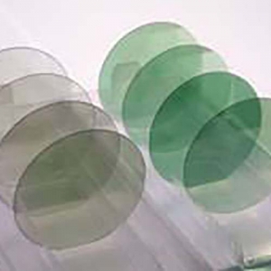
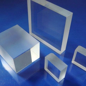
Applications: Used for grinding and polishing of sapphire substrate, LED substrate, sapphire window, optical crystal, watch dial, mobile phone glass panel, zinc selenide crystal
Introduction
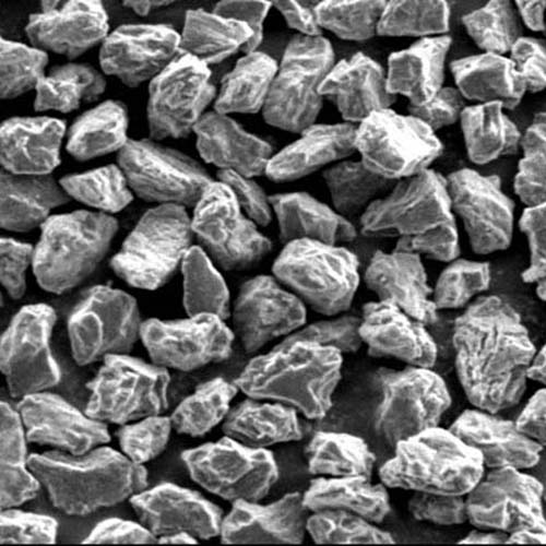
Crownkyn Superhard polycrystalline micron diamond is produced in a controlled explosion known as shock synthesis. The resulting grains feature a very rough surface morphology. Each polycrystalline diamond has many grinding surfaces. During the grinding process, the grinding parameters can be adjusted in time to perform grinding, fine grinding and ultra-fine grinding. And during the grinding and polishing process, it will automatically peel off in time and new micro cutting edges appear. This “self-sharpening” guarantees high precision, high efficiency of processing and will not damage the shallow surface layer.
Our polycrystalline micron diamond maximizes the productivity of grinding and polishing processes in a wide range of applications, meeting the demanding surface treatment requirements of various industries.
Features
- While maintaining a high cutting capacity, it can achieve a precise polishing effect, not easy to produce scratches.
- Compared with single crystal diamond, the particles have high toughness and self-sharpening.
- The product particle size distribution is concentrated, there will be no super large particles or super fine particles, and the impurity content is small.
- The product morphology is good, and needle-like or flake-like particles rarely appear.
Applications
1.Processing of precision ceramics.
2.Processing of silicon wafers in the IT industry, such as HDD components-recording heads.
3.Processing in the field of optical fiber communications, such as compound semiconductor wafers (II-Vi and III-Vs).
4.Precision processing of sapphire, silicon carbide and gallium nitride, the surface roughness Ra of which is less than 1nm.
5.Processing of optical lenses, such as optical and electro-optic crystals-lithium niobate and other oxide crystals, laser crystals-YIG, YAG.
6.Surface modification and machining of materials, such as hard brittle materials, hard alloys.
Type
| Size(μm) | MBDM | RVDM | PCDM | WSDM | PDM | PLM |
| 0-0.25 | √ | √ | ||||
| 0-0.5 | √ | √ | √ | |||
| 0-1 | √ | √ | √ | |||
| 0-2 | √ | √ | √ | |||
| 1-2 | √ | √ | √ | √ | ||
| 1-3 | √ | √ | √ | √ | ||
| 1.5-3 | √ | √ | √ | √ | ||
| 2-3 | √ | √ | √ | √ | ||
| 2-4 | √ | √ | √ | √ | √ | |
| 3-6 | √ | √ | √ | √ | √ | |
| 3-7 | √ | √ | √ | √ | √ | |
| 4-6 | √ | √ | √ | √ | √ | |
| 4-8 | √ | √ | √ | √ | √ | |
| 4-9 | √ | √ | √ | √ | √ | |
| 5-10 | √ | √ | √ | √ | √ | √ |
| 6-12 | √ | √ | √ | √ | √ | √ |
| 8-12 | √ | √ | √ | √ | √ | |
| 7-14 | √ | √ | √ | √ | √ | |
| 8-16 | √ | √ | √ | √ | √ | |
| 10-20 | √ | √ | √ | √ | √ | |
| 12-22 | √ | √ | √ | √ | √ | |
| 15-25 | √ | √ | √ | √ | √ | |
| 20-30 | √ | √ | √ | √ | √ | |
| 20-40 | √ | √ | √ | √ | √ | |
| 22-36 | √ | √ | √ | √ | √ | |
| 30-40 | √ | √ | √ | √ | √ | |
| 35-45 | √ | √ | √ | √ | √ | |
| 36-54 | √ | √ | √ | √ | √ | |
| 40-60 | √ | √ | √ | √ | √ |


