
1. Monocrystalline and polycrystalline silicon
Silicon is a hard and brittle material with a Mohs hardness of 6.5 and can be made into polycrystalline silicon and single crystal silicon according to the application. Monocrystalline silicon is a relatively active non-metallic element. This crystal has a basically complete lattice structure and is a good semiconductor material with a purity of 99.9999%. It is mainly used in the manufacture of semiconductor devices and solar cells. The manufacturing method of single crystal silicon (Fig. 1a) is usually to prepare polycrystalline silicon or amorphous silicon first and then grow rod-shaped single crystal silicon from the melt by the Czochralski method or the floating zone melting method.
Polycrystalline silicon (Fig. 1b) is a form of elemental silicon. When molten elemental silicon solidifies under supercooled conditions, silicon atoms are arranged in the form of diamond lattices into many crystal nuclei, such as these nuclei growing into crystals with different crystal plane orientations. grains and these grains combine to crystallize into polysilicon. Polysilicon is the direct raw material for the production of monocrystalline silicon and is the basic electronic information material for semiconductor devices such as contemporary artificial intelligence, automatic control, information processing, and photoelectric conversion. It is called “the cornerstone of the microelectronics building”.
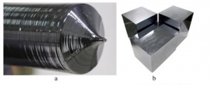
Fig.1 Monocrystalline and polycrystalline silicon
| Features | Monocrystalline silicon | polycrystalline silicon |
| Preparation Method | Czochralski method | cast polycrystalline method |
| Wafer size(mm) | 100*100 | 100*100 |
| 125*125 | 150*150 | |
| 150*150 | 210*210 | |
| Silicon resistivity(Ω·cm) | 1~3 | 0.5~2 |
| Wafer thickness(μm) | 200~300 | 220~300 |
| battery efficiency | 15~17 | 14~16 |
| Advantages | High conversion efficiency, low impurity concentration and high quality | High material utilization, low energy consumption, low cost and large size |
| Disadvantages | High material waste, high energy consumption, high cost and small size | Grain boundaries, grains, dislocations, micro-defects, high impurity concentration |
2. Manufacturing Process
The processing flow of single-crystal silicon mainly includes truncation → rounding → square cutting → flat grinding → slicing → chamfering → grinding plate → chemical etching → polishing and other steps. In contrast, polysilicon does not have the steps of truncating and rounding and only needs to be cut into squares and sliced after the preparation of the ingot.
In the process of preparing monocrystalline silicon and polycrystalline silicon from ingots (ingots) to chips, diamond tools of different uses are required to participate in the processing, and the processing precision is relatively high. The specific steps, corresponding tools and indicators are shown in Table 2.
| Machining Process | Diamond Tools for Application | Tool Indicators |
| Cutting | Diamond Circular Saw Blade/Diamond Band Saw | the circular saw blade of Diameter 200~600mm or the electroplated band saw blade of 0.5~1mm thickness |
| Rolling | Electroplated diamond wheel or sintered cup wheel | diamond grinding wheel of Diameter 300~400mm and diamond particle size is 250# |
| Slice | Diamond internal circular saw blade or diamond wire saw | Electroplated inner circular saw blade with a thickness of about 0.3mm or a diamond wire saw with a wire diameter of 0.12~0.16mm |
| chamfer | Diamond Grinding Wheel | resin or metal bond grinding wheel with diamond partical size of 250# |
| Polishing | Metal Bonded Diamond Grinding Wheels Resin Bonded Diamond Grinding Wheels |
2000# resin-based grinding wheel with diamond 2000# is used for rough polishing, and diamond grinding wheel with diamond 8000# is used for fine polishing |
| CMP chemical mechanical polishing | Diamond Dresser | Diamond electroplating, high temperature brazing, PCD dresser |
| Backside Thinning grinding | Metal Bonded Diamond Grinding Wheels Resin Bonded Diamond Grinding Wheels |
Diameter 150~250mm, diamond grain size 400#, bowl-shaped diamond thinning grinding wheel |
| Dicing | Diamond ultra-thin cutting disc | Electroplating cutting blade with thickness of 0.15~0.1mm or hot pressing sintering cutting disc with thickness of 0.1~0.5mm |
2.1 Wire-electrode Cutting
After the single crystal silicon ingot is pulled out, the head and tail are removed according to certain requirements, and after cutting to a certain length and processing the outer circle, the single crystal silicon rod must be cut into wafers of a certain thickness. The tools used were diamond internal circular cutting discs in the early days, and their cutting surfaces were flat and fine, but the production capacity was limited due to the slow speed. In order to increase production capacity, diamond saw blades and diamond wires are currently used instead of diamond cutting blades.
There are two principles of wire cutting, one is reciprocating swing cutting, and the other is one-way continuous cutting. In the reciprocating wire cutting, the metal wire and the workpiece are in an approximate point contact state, and the cutting is performed in an arc shape.
The one-way continuous wire cutting process can be free grinding, using stainless steel wire or molybdenum wire with a diameter of 0.15~0.3mm, and adding Sic or diamond micro powder to the cutting fluid. It can also be a fixed-abrasive grinding process, and 0.15-0.5mm plated diamond abrasive wire is used for cutting.
| Diamond Cutting Wire(mm) | Diamond Particle Size (μm) | Slit Size(mm) |
| 0.127 | 20 | 0.140 |
| 0.203 | 45 | 0.229 |
| 0.254 | 60 | 0.279 |
| 0.305 | 80 | 0.330 |
| 0.381 | 100 | 0.419 |
| 0.508 | 120 | 0.546 |
2.2 Wafer Chamfers and Rounded Edges
The outer edge of the wafer cut by the wire cutting or inner circular cutting saw blade is very sharp. In order to avoid the edge cracking affecting the wafer strength, destroying the surface smoothness and causing pollution to the subsequent process, It must be automatically trimmed the edge, shape and outer diameter of the wafer with special CNC equipment.
Monocrystalline silicon grinding surface and polycrystalline silicon grinding surface chamfering also need a lot of diamond grinding wheels. The processing process is divided into rough grinding and fine grinding. The diamond particle size is 120/140, W40, W28, W20, etc., and the main size specifications are 6A2-220* 65*130*5*5, 6A2 200*60*80*5*5, 11A2-100*28(40)*31.75(20)*5*5, etc.
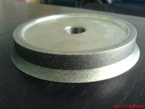
Diamond Grinding wheel for chamfer
2.3 Wafer backside thinning
The backside thinning grinding of wafers is divided into rough grinding and fine grinding. Coarse-grained diamond is used for coarse grinding, and fine-grained diamond is used for fine grinding.
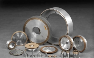
Grinding wheel for Edging
| Process | Diameter | Width | High | Diamond Size | Matrix |
| Coarse Grinding | Φ204 | 2-5 | 5 |
200/230 230/270 270/325 325/400 500/600 |
Elastomeric resin bond matrix Lubricating resin bond matrix Non-porous ceramic bond matrix Microporous ceramic bond matrix |
| Φ250 | |||||
| Φ300 | |||||
| Φ350 | |||||
| Fine Grinding | Φ204 | 2-5 | 5 | 1000#~3000# | Wear-resistant resin bond matrix Sharp resin bond matrix |
| Φ250 | |||||
| Φ300 | |||||
| Φ350 |
2.3.1 Application Characteristics
Thinning diamond grinding wheels usually include vitrified bond and resin bond, which are mainly used for the thinning and grinding of the backside or front side of the wafer in the manufacturing process of integrated circuits and discrete devices. The vitrified bond grinding wheel is mainly used for rough grinding. Resin bond grinding wheel is used for semi-finishing and finishing.
(1) Ultra-precision: The 2000# diamond grinding wheel with diamond powder 2000# is used to process an 8-inch silicon wafer, and the surface roughness Ra reaches 8nm. The diamond grinding wheel made of a special resin bond has surface roughness Ra≤2nm; parallelism (TTV)≤0.005mm; curvature≤0.5mm.
(2) High efficiency: the feed rate of the fine grinding wheel reaches 0.8m/s and 0.5μm/s (machine speed is 3600~4850rpm).
2.3.2 Product Characteristics
(1) Cup grinding wheel with diameter 114~444mm.
(2) The characteristics of the abrasive working layer: the narrow ring has a high thickness, the ring width is generally 2.5~3.5mm, and the thickness is 8~10mm.
(3) High requirements for manufacturing accuracy: dynamic balance accuracy≤G2.5; parallelism≤0.015mm; outer circle runout≤0.05mm;
(4) Ultra-fine particle size: 2000#(6~8μm), 3000#(4~5μm);
(5) According to the shape of the grinding wheel, it is divided into a whole cup shape, a shape with a water tank and a three oval shape with a water tank.
2.3.3 Key Technologies
(1) Low-temperature firing, high-performance vitrified bond suitable for diamond grinding wheels.
(2) Manufacturing technology of high porosity resin bond micro powder diamond grinding wheel.
2.4 Wafer Dicing
Wafer dicing requires the use of electroplating precision ultra-thin diamond saw blades, which are divided into two types in structure: one is an electroforming hub type cutting blade; the other is a circular hubless type cutting blade. This section briefly introduces the application characteristics, product characteristics and key technologies of electroplating bond for integrated circuit (IC) wafer dicing and high-precision ultra-thin diamond cutting wheels.
2.4.1 Application Characteristics
dicing blades, which are mainly used for micro-processing such as dicing, dividing or grooving of wafers in the pre- and post-processing of semiconductor integrated circuit (IC) and discrete (T°F) wafers. Its processing characteristics are as follows:
(1) Precision: the slit width error is less than ±5μm, and the slit collapse is less than 5μm.
(2) High speed: the operating speed is 30000~45000rpm.
2.4.2 Product characteristics
(1) Directly electroplating the diamond abrasive layer on the aluminium alloy substrate to form a hub-type cutting wheel.
(2) Ultra-thin: the thickness of the diamond abrasive powder working layer is 0.015~0.06mm.
(3) High precision: thickness accuracy is ±0.002~±0.004mm; hole (H) is 19.05+0.008+0.003mm; outer diameter is 55.60±0.05mm;
(4) Ultrafine diamond particle size: the smallest particle size is 0.5~2μm (30000#).
2.4.3 Key Technologies
(1) Uniform dispersion technology of ultra-fine powder abrasives.
(2) Electroplating solution formulation technology for low stress, high rigidity, high hardness and high flatness working layer.
(3) Technology to improve the bonding strength of coating and substrate.
(4) Precise removal technology of working layer supporting substrate after plating.
(5) Precision trimming technology for the outer circle and end face of the working layer.
(6) Non-contact detection technology of working layer thickness.
(7) Development of special equipment and devices, including high-efficiency precision electroplating devices and high-precision intelligent electroplating steady current power supplies.
2.5 Chemical Mechanical Polishing (CMP) Pad Dresser
Due to the development of ultra-large-scale integrated circuits (ULS) to highly integrated and multi-layer wiring structures, chemical mechanical polishing and planarization have become indispensable key processes for integrated circuits. It is not only the most efficient method to finally obtain a nanometer super smooth and damage-free surface in silicon wafer processing, but also an irreplaceable interlayer localized planarization method in the multilayer wiring of ULSI chips.The CMP process is used many times during wafer (chip) fabrication. At present, common dressers are (1) nickel electroplating type dressers, (2) high-temperature vacuum brazing dressers, (3) ceramic matrix ceramic bond dressers, (4) PCD dressers.
Taiwan KNIK company has developed a new type of PCD dresser. The PCD is sintered at 6GPa and 1350°C to form a trimmer carcass, which is then EDM machined into pyramids of specific size and shape. Pyramids arranged in a predetermined pattern are called ADD-Advanced Diamond Disks. Experiments show that ADD can make the polishing pad with high-density roughness, efficiently and uniformly polish the wafer, and double the lifetime (see Table 5).
| DiaGrid | ADD | |
| Flatness of Diamond | >50μm | <20μm |
| Polishing Efficiency | >50μm/h | >20μm/h |
| Participate in the Work of Diamond Grains | <10% | >90% |
| Broken Diamond Grains | >20% | <1% |
| Diamond Shape | irregular | Uniform symmetry |
| Diamond Crystal Angle | >1000 | <900 |
| Grinding Stress | large (torn) | small (cutting) |
| Polishing Temperature | high | low |
| Acid Proof | Not acid-proof | Acid proof |
| Pad Life | short | long |
| Dresser Life | short | long |
| Surface Roughness | random | uniform |
| Uniformity | low | high |
3. Conclusion
Since the development of integrated circuits (IC) is inseparable from the basic material silicon wafers, more than 90% of the world’s IC use silicon wafers. Silicon crystal slicing is at the front end of the entire process flow and is an important process in chip manufacturing. It has an important impact on the processing quality and cost of the substrate, and the quality of the slicing will inevitably affect the processing of subsequent processes.
In the manufacturing process of silicon-based semiconductor devices, grinding wheel grinding is mainly used for two purposes. On the one hand, it can be used for fine grinding of etched silicon wafers. The amount of silicon wafers removed during the polishing process; another use is to reduce the overall thickness of the silicon wafers before the dicing process. With the growing demand in markets such as smart cards and smart labels, the demand for thin, flexible silicon chips is also increasing, thus requiring more back grinding processes.
As the “teeth of industry”, diamond grinding wheel increasingly reflects its excellent performance in many emerging industrial material processing fields. With the improvement of raw material performance, serialization of product specifications, specialization of production equipment and standardization of testing methods, diamond tools will develop towards a higher level, and product quality will be significantly improved.

